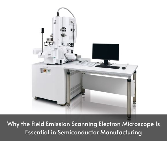
The Importance of the Field Emission Scanning Electron Microscope in the Semiconductor Industry
In the rapidly evolving semiconductor industry, the demand for miniaturization and increased performance necessitates advanced inspection and analysis tools. The field emission scanning electron microscope (FE-SEM) has emerged as an indispensable instrument, offering unparalleled resolution and precision.
Unlike conventional scanning electron microscopes, FE-SEMs utilize a field emission gun (FEG) to produce a highly coherent and focused electron beam. This results in superior imaging capabilities, enabling the detection of minute defects and variations in semiconductor materials.
Hansvue’s commitment to providing state-of-the-art FE-SEM solutions ensures that semiconductor manufacturers can maintain high yields and product reliability.
How the Field Emission Scanning Electron Microscope Detects Micro-Defects in Chip Fabrication
During chip fabrication, identifying and analyzing micro-defects is crucial to prevent failures and ensure device performance. The field emission scanning electron microscope excels in this area by offering high-resolution imaging that reveals sub-nanometer features.
FE-SEMs detect defects such as voids, dislocations, and contamination that might be invisible to other inspection methods. By providing detailed images of these anomalies, engineers can implement corrective actions promptly.
Hansvue’s FE-SEM systems are designed to integrate seamlessly into semiconductor fabrication processes, enhancing defect detection and contributing to overall manufacturing efficiency.
Field Emission Scanning Electron Microscope Use in Wafer Inspection and Layer Analysis
Wafer inspection and layer analysis are critical steps in semiconductor manufacturing, requiring tools that can provide detailed insights into the material’s structure. The field emission scanning electron microscope offers exceptional capabilities in this regard.
FE-SEMs enable the examination of wafer surfaces and cross-sections, allowing for the assessment of layer thickness, uniformity, and interface quality. This information is vital for ensuring that each layer meets the stringent specifications required for high-performance semiconductor devices.
Hansvue’s FE-SEM solutions are equipped with advanced imaging modes and detectors, facilitating comprehensive wafer analysis and supporting quality assurance efforts.
Advantages of Using the Field Emission Scanning Electron Microscope for Process Control
Maintaining tight process control is essential in semiconductor manufacturing to achieve consistent product quality. The field emission scanning electron microscope plays a pivotal role in monitoring and controlling various fabrication processes.
FE-SEMs provide real-time feedback on critical parameters such as feature dimensions, etch profiles, and material composition. This enables process engineers to make informed adjustments, minimizing variations and defects.
Hansvue’s FE-SEM systems are designed for integration into process control workflows, offering automation features and data analysis tools that enhance decision-making and process optimization.
Field Emission Scanning Electron Microscope Features That Benefit Semiconductor Engineers
Semiconductor engineers require tools that offer precision, reliability, and versatility. The field emission scanning electron microscope meets these needs through a range of advanced features:
High Resolution: FE-SEMs provide imaging at resolutions down to 1 nanometer, essential for examining fine structures.
Low Voltage Operation: Capable of operating at low accelerating voltages, reducing sample charging and damage.
Advanced Detectors: Equipped with detectors for secondary electrons, backscattered electrons, and X-rays, enabling comprehensive analysis.
Automated Functions: Features such as auto-focus, auto-stigmation, and automated stage movement enhance efficiency and repeatability.
Hansvue’s FE-SEM offerings incorporate these features, providing semiconductor engineers with powerful tools for research and development.
Unlike conventional scanning electron microscopes, FE-SEMs utilize a field emission gun (FEG) to produce a highly coherent and focused electron beam. This results in superior imaging capabilities, enabling the detection of minute defects and variations in semiconductor materials.
Hansvue’s commitment to providing state-of-the-art FE-SEM solutions ensures that semiconductor manufacturers can maintain high yields and product reliability.
Failure Analysis with the Field Emission Scanning Electron Microscope in Semiconductor Plants
When semiconductor devices fail, understanding the root cause is imperative to prevent recurrence. The field emission scanning electron microscope is a vital instrument in failure analysis, offering detailed insights into failure mechanisms.
FE-SEMs can reveal defects such as cracks, delaminations, and contamination at high magnifications. By analyzing these failures, engineers can identify process issues, material weaknesses, or design flaws.
Hansvue’s FE-SEM systems are tailored for failure analysis applications, featuring high-resolution imaging and analytical capabilities that support thorough investigations.
Selecting a Field Emission Scanning Electron Microscope for Semiconductor Applications
Choosing the right field emission scanning electron microscope involves evaluating several factors to ensure it meets the specific needs of semiconductor applications:
Resolution Requirements: Determine the necessary resolution based on the smallest features to be analyzed.
Sample Types: Consider the types of samples (e.g., wafers, cross-sections) and their preparation requirements.
Analytical Capabilities: Assess the need for additional analysis, such as elemental composition or crystallography.
Throughput: Evaluate the system’s speed and automation features to match production demands.
Hansvue offers a range of FE-SEM models with varying specifications, allowing customers to select a system that aligns with their operational goals and budget.
Conclusion
The field emission scanning electron microscope is an essential tool in semiconductor manufacturing, providing the high-resolution imaging and analytical capabilities necessary for quality control, process optimization, and failure analysis. Hansvue’s commitment to delivering advanced FE-SEM solutions ensures that semiconductor companies can meet the challenges of modern fabrication processes and maintain a competitive edge in the industry.